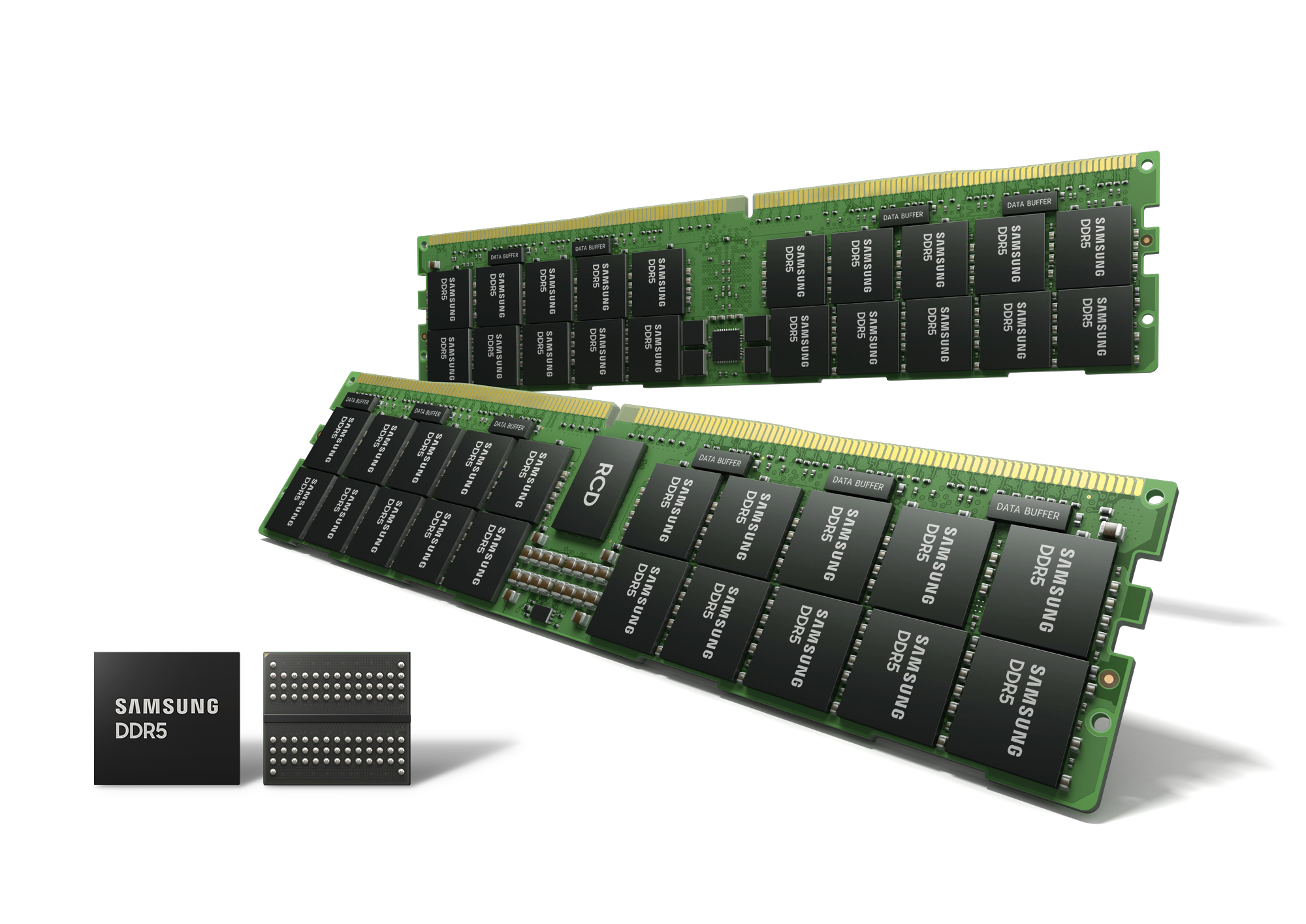
Out of the three large technology giants in the DRAM market, Samsung Electronics is by far the largest. Today, the South Korean company has announced that they have begun the mass production of DDR5 DRAM based on their 14nm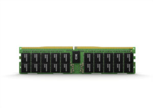 EUV processes.
Ever since the publishing of DDR5 specifications by JEDEC, manufacturers have been racing to announce their product stacks amongst the pandemic. EUV(Extreme Ultraviolet Technology) was used by Samsung during their shipment of the industry-first EUV DRAM last March, however now it’s being brought to DDR5. The number of EUV layers has been increased to 5 to deliver as Samsung quotes: “today’s finest, most advanced DRAM process for its DDR5 solutions.”
Samsung has managed to achieve high bit densities while enhancing overall wafer productivity by approximately 20% as claimed, and improving power efficiency. Samsung also advertises their latest product stack with bandwidth speeds up to 7.2 Gbps(gigabits per second), with expansion into the data center, supercomputer, and enterprise territory. Densities would range up to 24Gb as stated.
Jooyoung Lee, Senior Vice President and Head of DRAM Product & Technology at Samsung Electronics states : “Today, Samsung is setting another technology milestone with multi-layer EUV that has enabled extreme miniaturization at 14nm — a feat not possible with the conventional argon fluoride (ArF) process. Building on this advancement, we will continue to provide the most differentiated memory solutions by fully addressing the need for greater performance and capacity in the data-driven world of 5G, AI and the metaverse.”
Overall, I’m excited to see how the memory space continues to expand and innovate with DDR5, which brings some unprecedented changes and improvements over DDR4.